-
StatusCompleted
-
Status date2021-10-29
-
Activity Code4F.057
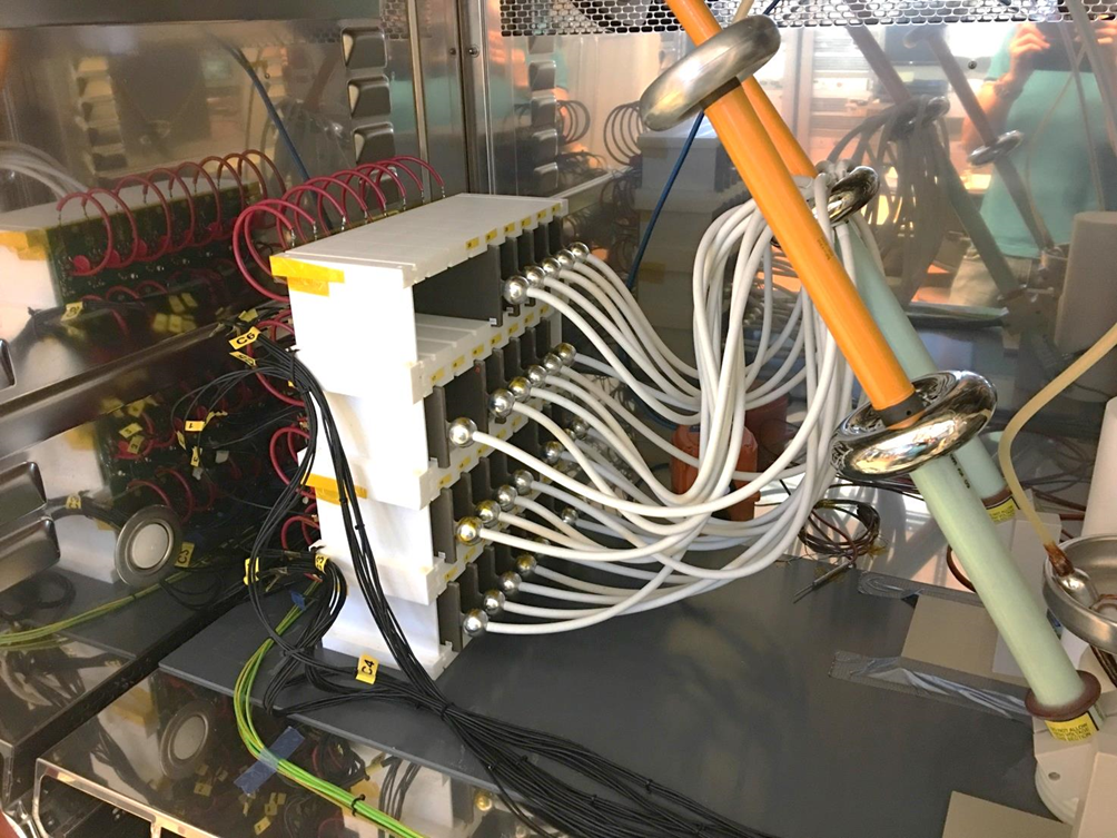
Although High Voltage Technology is a niche marked in space business, it is very important since it enables highly-efficient RF amplification with TWTAs, a significant payload element for a telecom spacecraft, as well highly-efficient generation of thrust per electric propulsion. Further, various scientific instruments rely on high voltage.
Pending on the equipment use, in space environment (and on the way there), voltages above 200V have to be considered as high voltage (see RD 3).
Communication TWTAs usually require voltages in the range of 4kV - 7kV, while most electric propulsion thrusters are fed with 300V … 2.000V, pending on the thruster technology.
A comparison of standards for HV on PCB designs either did not exist jet or differ in the distance / material thickness rules (see chapter 4). Further, the parameters and sources, how the rules (if existing) were determined are not available.
Heritage and current designs either avoid high voltage on PCBs or are based on qualified heritage designs, where the true margin for lifetime until electrical breakdown is not known.
All together shows the urgent need for research in this field: Determination of design rules for HV-PCBs for different space-environment compatible coating-, potting-and PCB-substrate-materials, based on lifetime measurements under known parameters enables better prediction of design durability.
Main challenges, experienced during the study, were test equipment fails and disturbances due to the electrical breakdowns to the data acquisition system and unexpected long duration to test all the samples.
N/A
N/A
N/A
In the beginning, a plan was created to define the sample variants and different PCB layouts. Further, the test strategy has been defined in the Study plan. After release of this plan in the Study Plan Review, the detailed samples and potting mould design was conducted and released with the Manufacturing Readiness Review (MRR). This was followed by the samples production and delivery to the test Facility (HV-Testlab @ ESTEC). Finally, the tests results have been analysed and summarised in the final report.
All sample production, testing and results analysis is completed.