-
StatusCompleted
-
Status date2016-06-23
This activity aims at the development of a fully European source of high performance monolithic switchable VCO bank based on SiGe technology.
The objective of the activity is the design, manufacture and test of two alternative chip-on-board (COB) low-noise monolithic switchable VCO banks covering a frequency range from 1.25 to 3.3 GHz.
Contradiction between requirements can be mitigated by a monolithic switchable VCO bank and/or with sub-band switching with each VCO. This requires a good level of integration which recalls the use of RF BiCMOS SiGe process.
The real strength of SiGe lies in its ability to integrate analogue, RF and digital in a single chip and also in low 1/f noise (due to the very low 1/f device noise corner frequency in SiGe HBT technology), a necessary feature for low phase noise VCO’s.
The SiGe technology allows realisation of monolithic frequency dividers that can be added for very wide-band coverage over several octaves.
Radiation hardened by design.
SiGe VCO chip consists of the two VCO cores (PMOS and BJT), digital control block, voltage reference and low-dropout voltage regulators.
VCO tuneable frequency range is 0.83 GHz - 3.48 GHz.
PMOS VCO SSB Phase Noise @ 3.1 GHz: -50.3 dBc/Hz (1 kHz offset), -83.5 dBc/Hz (10 kHz offset), -112.5 dBc/Hz (100 kHz offset), -135.5 dBc/Hz (1 MHz offset), -150.8 dBc/Hz (10 MHz offset),
Three tuning parameters: Analog tuning: 1-8MHz/V, Coarse digital: 3-15MHz/V and Fine digital: 0.1-8MHz/V.
Analog tuning voltage is between 0-2.5V.
VCO is controlled via 4-wire serial peripheral interface (SPI).
Operational temperature range: -40°C…+85°C
Supply Voltage 3.3 (PMOS) and 5.5V (BJT).
Silicon Area (for IP) is 1300 x 2500 mm2.
SYSTEM ARCHITECTURE
The Fig 1 shows general architecture and layout of the VCO chip. VCOPMOS is situated on the top while the VCOBJT is placed on the bottom. For short and straightforward wiring, Digital control is placed in the middle. The output buffers are placed as close as possible to RF output pins. The die size without scribe line is approximately 3.0 mm x 3.1 mm.
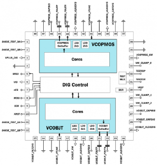
Figure 1: VCO chip general architecture and layout.
Fig 2 displays picture of the fabricated chip and Fig 3 shows the evaluation board.
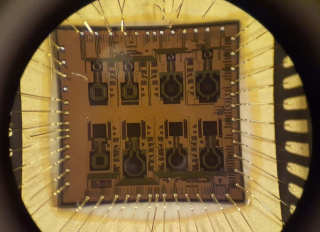
Figure 2: Fabricated chip, package opened. ©Sami Sipilä, CoreHW
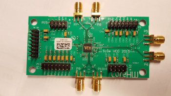
Figure 3: SiGe VCO evaluation board. ©Sami Sipilä, CoreHW
In the Phase 1 the project carries out analyses of the literature and existing technologies, suggestions for the VCO topologies will be given and additional solutions will be explored. Modelling of all functional blocks and parts of the switchable VCO bank and model validation will be carried out. The models will allow for quantitative prediction of the SiGe VCO block performance.
Phase 2 will focus on design, manufacturing and testing of two VCO blocks.
All major technological development steps are documented and followed by review meetings. Two type of SiGe VCO blocks are manufactured and tested.
Project completed:
- All implementation and integration work is completed.
- Measurement results deduced, evaluated and validated.
- Testbed (evaluation board) delivered to ESA.
Final presentation including demonstrations with the testbed has been given.