-
StatusCompleted
-
Status date2013-04-09
Aim of the FENICE project is to develop a Satellite AIS receiver Prototype, able to decode and detect the AIS messages transmitted by the ships covered by the Antenna FoV of a SAT-AIS LEO satellite, fully compatible with both existing and future AIS terrestrial transponders. The proposed implementation is fully flexible and covers both the case of on-ground and on-board processing, as well as the deployment of different antenna subsystems.
The design and development of the prototype allowed assessing in detail the performances and complexity of the innovative demodulation algorithms, implemented on the target device. A dedicated Testbed, able to generate the required AIS signals, was also developed.
The assessment of the performance and complexity of the processing was achieved by implementing on target FPGA the enhanced algorithms and technologies originally proposed by ESA, and further improved during the FENICE project. Thanks to these innovative demodulation algorithms and architecture, FENICE demonstrated to outperform all the known space-based AIS receivers.
The results of the project demonstrated that the FENICE receiver provides an excellent solution both in terms of signal processing and in terms of technology to cope with the extremely challenging C/I expected over the AIS channels as seen from the satellite.
In parallel, a complete SW Model of the FENICE receiver has been developed, to be used for payload characterization tests in the frame of SAT-AIS Phase B1 projects, and for subsystem performance evaluation in the frame of ESA CPA activities.
The items produced in the frame of the described project will be developed up to TRL 4 (Component and/or breadboard validation in laboratory environment).
The novel aspect of the FENICE device lies in the combination of two technologies (digital signal processing and antenna) to optimize the performance of the probability of detection of AIS messages sent from the ships and received at a LEO satellite.
In fact, the FENICE AIS receiver for satellite AIS services aims at providing an innovative solution both in terms of signal processing and in terms of technology to cope with the extremely challenging C/I expected over the AIS channels as seen from the satellite.
Nowadays, the market of an AIS receiver for satellite services is at an early stage. At present there were only four potential manufacturers in the world who demonstrated interest in developing AIS receiver for satellite services: two are European and two are American.
The FENICE team is the only Italian team mentioned in recent activities relevant to the development of applications of the AIS receiver technology, specifically thanks to ESA Satellite based AIS feasibility Study in which CGS is involved for the space segment and CNIT for the AIS receiver algorithms design.
In this context the FENICE team has good chances to reach a leading position in Italy and Europe, thanks to the excellent results obtained during ESA AIS projects.
A strategically important technology shall be therefore available for the European and Italian space community, able to provide a pre-operative effective service in the framework of the EU-ESA initiatives on this subject and an innovative, flexible product in the commercial AIS market.
The effective innovation and quality of space AIS services will largely depend on the performance of the AIS receiver: The FENICE receiver is, therefore, a key product of the space AIS system.
From the performance characterization carried out to date, it is evident that the FENICE demodulation algorithms outperform all other competitors on the market, and should then be taken into strong consideration for the implementation of a high-performance SAT-AIS system.
FENICE project foresees to:
- Design and develop AIS receiver, including the Digital Section and the RF/IF chain (Prototype),
- The design and development of an AIS RF channel simulator (Testbed).
The design has been carried out with its future QM implementation in mind: several design choices have been performed taking into account compatibility and portability issues versus mainly space devices in order to minimize redesign activities.
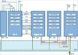
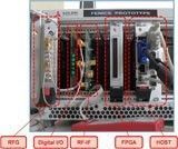
An approach based on 3U cPCI boards has been selected for Prototype implementation. The developed architecture includes Modules made of mixed COTS and Custom boards, all hosted on a commercial cPCI chassis with a dedicated power supply unit.
Modules are organized as follows:
- RF-IF Module, composed by:
- RF-IF Front-End (developed by CGS from scratch, hosting the Analog-to-Digital converters);
- Digital I/O (based on CGS-proprietary general-purpose board, performing digital signal conditioning and buffering);
- Radio Frequency Generator (providing Local Oscillators and master clocks).
- Digital Module: an FPGA Board equipped with target Virtex5 device (selected among those having a space-grade counterpart), for VHDL implementation of the advanced demodulation algorithms.
- Host Computer, for prototype management (through dedicated Application SW) and interface to Testbed.
A block diagram and the physical realization of the Prototype are shown in the following figures.
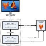
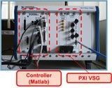
The main task of the Testbed is to verify and validate the performances of the AIS digital receiver. It is based on the PXIe-5672 vector signal generator by National Instruments, and is able to generate test case inputs in manual mode (for specific tests) and automated mode (for statistical performance characterization).
The project was organized into four main work packages:
- System Consolidation, where the requirements have been defined, both for Prototype and final Payload. The algorithms and the architecture of the AIS receiver have also been specified in this phase.
- Design, where the Prototype (RF-IF section and Digital section) and the Testbed have been defined. Translation of the demodulation algorithms from fixed-point C-code to VHDL has been carried out.
- Manufacturing, where the Prototype and the Testbed have been manufactured and integrated. FPGA netlist has been delivered and tested on the target device. Functional tests on each subsystem have also been carried out at the integration level.
- Testing, where the performances of the demodulation algorithms as implemented into FPGA have been extensively characterized.
The FENICE project is COMPLETED.


