-
StatusCompleted
-
Status date2011-03-31
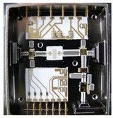
The aim of the present project is to identify the improvements obtained by the introduction of GaN MMIC technology in terms of survivability and linearity of the RF chain. In the frame of this project, LNAs and Mixers have been designed and fabricated in order to fabricate 3 RF Front-Ends (RFFE). The RFFE demonstrators allowed to demonstrate these improvements and the interest of using GaN technology for the receivers for secure communications.
This activity has aimed at design, manufacturing and testing of three GaN-based receiver front-ends at C, Ku, and Ka bands, respectively. The most important design goal has been in the robustness i.e. in high power handling while still maintaining good noise figure that is comparable to GaAs-based receiver front-ends.
The first part of this project was first of all dedicated to the design, manufacturing and testing of GaN-based LNAs and Mixers. Two iterations have been carried out to realize these chips and to optimize the power handling of the LNA and the linearity of the Mixer. The second part was devoted to the design and manufacturing and testing of the RFFEs using the GaN-based MMICs to evaluate the robustness of the receivers.
The Low Noise Amplifier and the Mixer of the RFFE chain have been developed in GaN MMIC technology. The other part, such as filters, will be in classical technology such as used nowadays. The Wide Band Gap technology has been used in order to improve robustness for the Low Noise Amplifier Stage and in order to improve both robustness and linearity for the Mixer stage. The RFFE demonstrators showed very good robustness capability using these GaN-based technology.
The Wide Band Gap technology has made a remarkable breakthrough in the World for the power application and with the announcement of commercially available transistors.
Improvements are obtained in terms of power density, maximum junction temperature and breakdown voltage. Moreover, several studies show that this technology can be advantageous in the case of low level stage.
The receivers need both low noise amplification and less distortion. Low noise, high breakdown GaN HEMTs in amplifier front ends could reduce the need for diode limiters as protection against RF overstress. The high power capability of this technology could be directly translated into the ability to handle a high input power or energy spike without failure in the receiver. Also, the comparison between GaN and GaAs technologies shows that Wide Band Gap devices allow better dynamic power range and inter-modulation behaviour.
In microwave applications, the GaN technology is typically used for power amplification. However, the results of this activity demonstrate that GaN be very useful in receiver applications, too, where good noise figure and robustness are required simultaneously. At MMIC level, the fabricated LNAs and Mixers demonstrated good performance especially in terms survivability and linearity.
At RFFE level, the robustness performance has been addressed by means of step stress test. The stress applied to these demonstrators was much higher compared to classical GaAs-based space equipments. The results obtained showed very good capabilities in overdrive conditions because no degradation in the important parameters has been observed.
In this consortium, several partners are involved and are in charge of different tasks and each task is reported in technical reports. The project progress is divided in 4 phases :
Phase 1
- Preliminary Design
- GaN Process Selection vs Current GaAs Performances
- Description of IAF Processes
- Preliminary Spec. And Baseline Design
- RFFE Preliminary Designs
- LNA MMIC Preliminary Designs
- Mixer MMIC Preliminary Designs
- MMIC Foundry Design Support
Phase 2
- First Iteration
- RFFE Detailed Designs
- First LNA MMIC Designs Iteration
- First Mixer MMIC Designs Iteration
- First RUN Manufacturing and Test
- First LNA MMICs on Probe Validations
- First Mixer MMICs on Probe Validations
- RFFE Breadboards Manufacturing
- RFFE Breadboards Validation and Test
Phase 3
- Second Iteration
- Second LNA MMIC Designs Iteration
- Second Mixer MMIC Designs Iteration
- Second RUN Manufacturing and Test
- Second LNA MMICs on Probe Validations
- Second Mixer MMICs on Probe Validations
- RFFE Demonstrators Manufacturing
- RFFE Demonstrators Validation and Test
Phase 4
- Overall RFFE Synthesis
- Design Documentation Completion
- Assessment of GaN Foundry
This activity started in October 2007.
All the tasks have been realized and the Final Revue was held on the 9th of December 2010 at ESTEC, The Netherlands. All presentations can be downloaded from the documentation area on Daptiv Webpage.


