
-
StatusCompleted
-
Status date2019-11-21
-
Activity Code4F.111
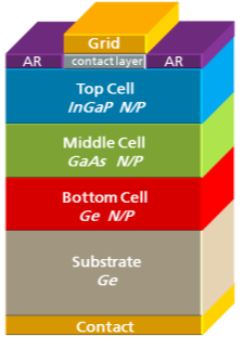
The main objective of the NanoCoat project is to develop a set of innovations based on functional surface coatings aimed at increasing the power conversion efficiency of present and next generation multi-junction (III – V) solar cells (MJSC) for space applications. An increase in power conversion efficiency of at least 0.5% is expected for standard and reduced thickness MJSC considered. This goal will be pursued by engineering for both of them a broadband antireflection coating (wavelength from 250 to 1800 nm), better surface and edge passivation (front and rear) and more efficient electrical contacts (front and rear).
For next generation MJSC with reduced Ge substrate thickness (≤ 80 μm) and hence higher specific power, W/g, the Nanocoat project will introduce ad hoc photonic structures capable of increasing the optical path of IR photons with respect to the standard flat metallisation approach. Such an ambitious objective is of outmost importance as it provides for the potential for a sharp rise in the capability of harvesting Energy in space, through a more efficient exploitation of the solar spectrum.
Innovative materials are explored: wide band gap materials as components of a multilayer broad-band ARC and passivation layers for the front of the MJSC; unconventional conductors for front and rear electrical contacts; back surface passivation layers and photonic structures to increase the optical path of IR photons in thin TJSC.
Sputtering is the reference thin film deposition technique since it is developed in industrial settings, nevertheless less conventional techniques (Pulsed laser deposition and pulsed electron deposition), are tested for their unique ability to deposit highly adherent, dense and low roughness coatings of a variety of materials at low substrate temperature.
The efficiency increase of at 0.5% is pursued developing both of them a broadband antireflection coating with three different approaches, a better surface and edge passivation and more efficient electrical contacts. In particular the coatings developed in Nanocoat project integrate passivation layer for minimizing the surface recombination velocity at the front and back surfaces of the MJSC. New approaches for the reduction of the reflection losses are theoretically and experimentally studied using as baseline CESI space triple junction solar cells CTJ30 already qualified as standard and thin version.
These results are followed bearing in mind the requirements of space solar cells in terms of radiation resistance, industrialization and cost.
Two new antireflection coating (ARC) designs demonstrate to be superior with respect to standard CESI antireflection coating design: a triple-layer structure and a gradient-index structure. Both structures are fabricated on top of 2x2 cm2 solar cells, in order to assess their optical and electrical performance before the scale-up towards 4x8 cm2 solar cells. In the new ARC designs the surface and edge passivation are provided by the conformal deposition of Nb2O5 (both for the triple-layer and the gradient-index ARC) a wide band-gap transitional metal oxides. The pulsed laser deposition technique ensures that both the surface and the edge of the solar cell substrates are covered with high-quality films during the deposition process.
High quality copper deposited by sputtering, as an inexpensive alternative to the current gold-capped silver for the front and back metallic contacts, is investigated.
The triple-layer ARC design is determined using optical simulation software suitable to simulate both the electrical and the optical behaviour of a multi-junction solar cell. Preliminary investigations allowed to define Nb2O5 / Ta2O5 / SiO2 as the most promising architecture to improve the standard ARC. Nb2O5 film is deposited by Pulsed Laser deposition (PLD) meanwhile Ta2O5 and SiO2 layers are deposited through an industrial electron-beam (physical vapour deposition).
As alternative approach a gradient-index ARC design is designed by IIT calculating the best-performing refractive index profile that minimizes the reflectance in the broadband 300-1800 nm spectral range. In this case the resulting structure is a 1500-nm-thick Nb2O5 film obtained by carefully controlling the porosity of the nanostructured film during PLD growth deposition.
MS1: Selection of processes, materials and tools
MS2: Material Readiness Review with ESA to discuss and consolidate the PID before the manufacturing of solar cells
MS3: Test Readiness Review with ESA to discuss and consolidate the Test Plan to be carried out during the prequalification test campaign.
MS4: Experimental process evaluation: proof of the coatings quality and identification of the suitable processing path on the basis of the evidence of the lab performances. Manufacturing and testing solar cells. Process flow and Cost Analysis
The triple-layer ARC structure has its best optical response in the 400-900 nm spectral range whereas the gradient-index ARC provides an overall reduction of the total reflectance. The measurements on CTJ30 CESI solar cells under a continuous light dual source solar simulator show a significant increase in the electrical performance of the device coated with the two new ARC structures with respect to the standard. The efficiency increase is achieved. The triple layer ARC is upgraded for standard 4x8 cm2 solar cells. Several devices are successfully tested showing no degradation of the electrical parameters after irradiation, thermal shock and humidity & temperature tests.
