-
StatusCompleted
-
Status date2015-05-13
-
Activity Code4D.020
The design of PCB (Printed Circuit Board) is constrained by the thermal management of the most dissipative components. Indeed, as only conductive heat transport is available, it is required that the most dissipative components be placed close to the PCB thermal interface. Moreover, conductive links, as thermal straps, are used in order to insure the specified temperature on high dissipative component (close to 10 W).
Less dissipative components are pushed away to hotter zones of the PCB leading to degraded reliability figures and a lay-out not optimized in terms of performance.
The recent progress made in the technology of Loop Heat Pipes (LHP), where stable heat transport can be achieved with input powers of 10Watts or less, make it a potentially interesting technique to relieve the design of PCB for the constraints above.
The application reference case is a cooling of electronic devices in Small Modular Processor application. The objectives of this activity were to identify the most suitable LHP technology, to define and justify the solutions retained, to manufacture, integrate and test the models and to compare to the initial reference design.
The major design driver requirements are described hereafter:
- Qualification evaporator temperature range : [-50°C +95°C]
- Power range : main dissipative elements: [5-15]W, second dissipative components: [3-5]W
- Envelope / IRD / accommodation : evaporator height and line routing (bends)
- Mechanical Environmental loads (shock)
- Ability to start up at temperature of -40°C / no overshoot
- Thermal performance : Ctot 1W/K (x3 better than copper strap)
- Condenser heat sink max temperature 62°C
- Mass (80g)
- Integration sequence / handling / mounting/ dismounting
Interfaces (flatness/stiffness)
The main technical improvement is a gain of close to 15°C on FGPA (main dissipative components) maximum temperature by comparison to classical thermal design (using thermal copper strap) at high power (15W at evaporator level, 5W at Hex level).
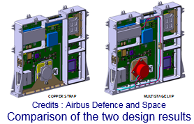
The multistage architecture, which efficiency has been demonstrated by test, allows cooling a secondary heat source. On the breadboard, the secondary heat exchanger proved useful for cooling the power supply. Thus, the concept can be adapted to various PCB design.
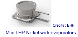
The evaporator (Nickel wick) is a generic item that has already been qualified and flight proven in the frame of telecom spacacraft projects according to the ECSS-E-ST-31-02C (Two-phase heat transport equipment ECSS).
In order to be compliant to max. temperature level to 95°C (70°C on generic item), to fit with SMP interface and to improve thermal contact, a custom evolution has been proposed with a larger and thicker LHP saddle.
Thermal performance has been assessed on the following aspects:
- Temperature expected for different heat applied
- Condenser dimensions check, with first condenser and second condenser regarding the subcooling aspect purpose
- Influence of parasite fluxes at lines level on LHP behaviour
- Multi-stage behaviour check with no plug slug regime expected, hence confirming stable expected functioning of the LHP.
- Comparison to thermal straps use

SYSTEM ARCHITECTURE
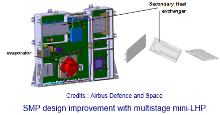
The objective of the design is to use a capillary loop heat Pipe (LHP) in order to evacuate heat from electronic components. The mini LHP Nickel wick developed by EHP and Airbus DS is used and implemented on the main dissipative component of the SMP: FPGA.
The multi stage (Airbus DS patented) concept is used in order to insure heat transfer from a secondary heat sink zone. The main multi stage principle is to evacuate a part of heat from the main dissipative component at evaporator level in a primary condenser and to go through a secondary heat exchanger to evacuate heat from a secondary heat sink (with lower power).
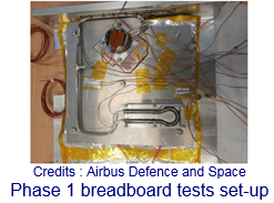
The project has been divided into 2 phases:
- A 18 months phase 1 aiming at designing the concept and performing tests on a breadboard
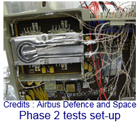
A 12 months phase 2 aiming at adapting the concept on a real case PCB resulting on a EM which been tested.
The activity is COMPLETED.
Phase 1 tests have been successfully performed: the test has been done with PCB/SMP and interfaces representative plate. All test objectives have been met in terms of start-up, inhibition, LHP performance characterization, multistage functioning in vacuum.
Phase 2 tests have been successfully performed: SMP has been retrofitted with the mini-LHP in multistage configuration. Configurations with copper strap and with LHP have been tested.