
-
StatusCompleted
-
Status date2021-03-23
-
Activity Code5C.397
The project aims at building a frequency synthesizer chip that is suitable for various applications, such as on-board clock generation, RF frequency synthesis, clock cleaning and jitter filtering. To this end, the rad-hard frequency synthesizer chip can generate a wide-range of output clock frequencies (1 MHz ~ 2.5 GHz). It has extremely low jitter (0.46 ps rms), and outstanding phase noise performances (<-99 dBc/Hz at 100 kHz offset frequency). It also features a high resolution (1 ns) PWM signal generator that provides optimal control for switching power supplies. The targeted power consumption of the chip is below 100 mW.
The ASIC is hardened against both total-ionizing-dose (TID) effects and single-event effects (SEEs), such as single-event latch-up (SEL) and single-event upset (SEU). The design target for TID hardness is taken to be greater than 100 Mrad, to cover applications in space, nuclear and high-energy physics. The targeted SEL/SEU tolerance is set to be higher than 120 MeV·cm2/mg. Radiation-hardened-by-design techniques at all levels (e.g., transistor, topology, circuits, and layout) are employed to achieve these ambitious goals.
Production of a silicon prototype of the frequency synthesizer system-on-chip in the chosen CMOS process is part of the project scope, as well as testing in both lab and relevant radiation environments.
The added value of the outcome of this project towards future customers spreads out over various aspects, in particular the technical specifications and the multi-use of the product. The low noise, high radiation tolerance and wide frequency range together with the additional high duty-cycle resolution pulse-width modulator functionality makes this whole project challenging.
Today’s available rad-hard frequency synthesizers all have a TID specification of a few hundred kRads (Si) and SEL specification around 100 MeV∙cm2/mg. This makes them suitable for systems used in near earth-orbit space missions. However, there is a growing demand for electronics that can withstand more harsh radiation environments. An example of this is the need of electronics for deep space exploration that can withstand a TID level of at least 1 Mrad. The proposed synthesizer has a target TID specification of more than 100 Mrad which is necessary for being functional in extremely harsh radiation environment. The SEU tolerance specification is targeted at more than 120 MeV∙cm2/mg.
Currently, companies who produce switched-mode power supplies experience difficulties in improving power efficiency of their products, because the lack of a high-resolution PWM signal. This project tackles that problem by using a digital PWM generator driven by the very high frequency synthesized clock (up to 1 GHz) resulting in a duty cycle resolution of 1 ns. Including this feature in the design makes this chip very attractive for power applications.
Finally, the proposed prototype ASIC is produced in a commercial CMOS technology. Many of the rad-hard IP blocks can be reused for development of future space grade ASICs.
This frequency synthesizer chip features:
- A reduced bill of materials thanks to an integrated loop filter, integrated RF oscillator and a single voltage rail operation when using the CMOS output.
- Integrated crystal oscillator amplifier and tuneable capacitance.
- A wide output frequency range of 1 MHz – 3 GHz.
- Excellent phase noise performance of -99 dBc/Hz at 100 kHz offset with 2.5 GHz carrier and an integrated jitter of 460 fs.
- User selectable input reference: using the crystal oscillator or an external clock generator / master clock.
- A multitude of supported external reference signal levels:
- 1.2/1.8/2.5/3.3 V, single-ended or differential.
- User selectable output signalling: LVCMOS-12 or LVDS-25 levels.
- A complementary PWM output with 1 ns pulse width control.
- Serial control and diagnostic interface.
- Measured radiation tolerance:
- > 1 kGy TID
- > 60 MeVcm2/mg SEL/SEU

Typical frequency synthesizer application drawing.
(credits go to MAGICS Instruments)
On the reference side, a user can provide its own system or master clock via the external reference input or use the on-chip tuneable crystal oscillator that works with an external quartz crystal.
The reference clock serves as an input for the wideband frequency synthesizer. The synthesizer is fully integrated and does not require external components. The chip output can be generated as an LVCMOS signal up to 200 MHz or as an LVDS signal up to 3 GHz.
The chip also contains supporting analog circuitry, like a bias generator, LDO’s and a temperature sensor.
A serial interface allows accessing and programming of the chip. It can also be used to enable a diagnostics mode
- Architecture definition and block topologies.
- Ends by mid-April 2019.
- Chip design phase.
- Synthesizer development by KU Leuven Advise team.
- Full-chip development in parallel, performed by Magics.
- Intermediate design reviews.
- Prototyping phase.
- Starting February 2020.
- Chip fabrication and packaging.
- Test plan preparation for characterization and radiation assessment.
- Electrical characterization.
- The chip performance is tested under all operating conditions.
- Radiation assessment covering the rad-hard specifications.
- The project closure date is February 2021.
The project is completed.
A prototype frequency synthesizer ASIC is achieved.
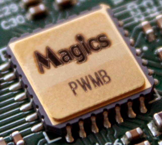
Prototype frequency synthesizer in a CLCC-28 pin package.
(credits go to MAGICS Instruments)