-
StatusCompleted
-
Status date2016-12-19
-
Activity Code5C.169
The project has achieved the following major objectives:
1) Address the application scenarios of most up-to-date challenging satellite communications;
2) Set the specifications for the flexible onboard processors suitable to the selected scenarios;
3) Execute a comprehensive survey for the ADC and DAC space qualified devices capable to directly digitize and synthesize RF frequencies up to Ka band;
4) Address the companion devices to push to the higher RF frequency limit the receive and transmit frequency, via e.g. sample and hold devices to be associated to ADCs and the highly integration scale Gilbert cell mixers to be associated to DAC;
5) Define an analytical modelling for the non-linear behaviours of the ADC and verify it with tests;
6) Design and manufacture a triple chain demonstrator to assess the developed concepts and European data converters capable to directly handle L band with only digital electronics:
7) Execute a test campaign characterizing the absolute and relative performances of the three RF to digital and back to RF chains;
8) Develop a higher order modulation BER tester to characterize the performances in a state-of-the-art air interface scenario.
Direct handling in digital of L band signals is now being deployed in competitive products.
The project has successfully fronted the challenges associated to complex high speed design both for boards, ancillary electronics, and digital processing capable to match the critical requirements. Novel data conversion components, that were initially released as engineering samples, needed acquisition of competences and – among other issues - verification of mutual synchronization procedures as well as accurate parameters alignment. Last but not least, the selection and procurement of state-of-the-art test instruments has been one of the crucial efforts of the demonstrator test campaign. For the complex ADC analytical model validation, high cost test signal generation and measurement instruments have been required.
The developed hardware building blocks, the associated algorithms and control logic constitute a valuable means for competitive onboard units production. Power consumption reduction, size and weight minimization are certain to be achieved by use of the RF2D and D2RF solutions.
Reduced manufacturing costs and minimal testing time are being achieved for the products employing the developed techniques.
Accurate characterization of absolute and relative performances are enabling implementation of beamforming products that were extremely difficult to manufacture before.
Products benefitting of the developed hardware building blocks are all of the wideband communications products, that simultaneously exploit both the wideband potential and the complete removal of analog conversion mixers and frequency generation units. The repeatability of individual chain performances are key enablers for multi-chain products including multibeam satellite communication systems. Also narrowband onboard processors will benefit of the achieved reduction in power consumption, size and weight. The solutions, initially developed for communications, are enabling technologies also for Earth Observation payloads, both for the onboard instruments signal generation and processing units and for the data transmissions systems. That applies also for Navigation.
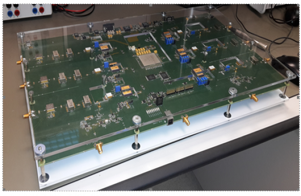
The figure shows the core of the demonstrator developments: the board is a multi-channel module able to acquire the input signals using the three ADCs, to process and to re-transmit the acquired data using the three DACs. An external unit, a Personal Computer, is devoted to the demonstrator configuration and controls all of the functions of the demonstrator internal modules. The board is also equipped with an FPGA for the signal processing and to control the internal and external module interfaces, the input signals acquisitions, the output signals generations and the memory. The architecture includes the following main blocks: 3 Front-End chains including 3 ADCs; one FPGA, 3 Back-End chains with 3 DACs, a clock distributor. The analog chains (input and output) perform the analogue signal conditioning: filtering, amplification and differential AC coupling. The main elements of these analog chains are the low pass filter, the BALUN and the RF Amplifier. the following components are used: o EV10AS180 Analog-to-Digital Converter supplied by E2V o EV12DS130 Digital-to-Analog Converter supplied by E2V The three ADCs and the three DACs are accurately synchronized in order to handle the three Input and Output RF Chains with fixed and deterministic phase matching.
The project has encompassed a System Specifications Review, in which both application scenarios and demonstrator specifications have been reviewed. Contextually a comprehensive review of the existing technologies has been executed, setting the baseline for the preliminary design. In this phase all of the ADC and DAC technologies have been addressed, with particular attention to the European technologies. Companion devices have been revised, to push to the higher RF frequency limit (Ka band) the receive and transmit frequency, via e.g. sample and hold devices to be associated to ADCs and the highly integration scale Gilbert cell mixers to be associated to DAC.
Afterwards, a preliminary design has been brought to the attention of ESA for approval in the PDR.
The Test Readiness Review has been executed to verify suitability of the proof of concept demonstrator as well as the innovative Software Radio Based BER meter, for high order modulation.
Finally the test campaign has been executed and part of it repeated at the presence of the customer ESA.
The current activities are encompassing the exploitation of the developed building blocks that have passed the feasibility study phase to achieve successful demonstration. TAS-I is moving from the achieved demonstration to employment in of the developed building blocks EQMs within the military communications product arena with cross fertilization towards the Earth Observation and Navigation products domain.
Tests have been executed both in maximum wideband mode and including within the FPGA the IP core of a TAS-I catalog product for military satellite communications to pave the way to the EQM.
The project has been completed.